About us

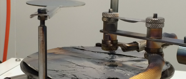
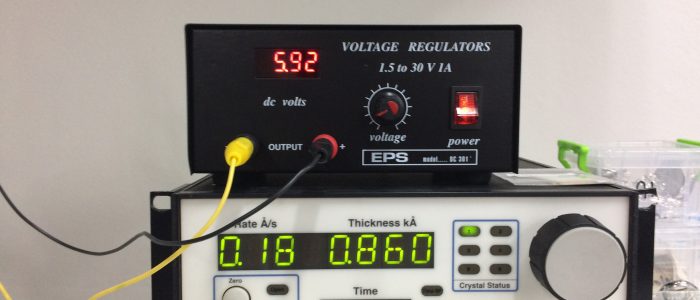
  • Resistive thermal evaporator


Dr. Supasai’s research focuses on nanostructured materials for advanced optoelectronic and photovoltaic applications, with particular emphasis on materials design, interfacial engineering and device physics. A central theme of her work is the development of hybrid and inorganic perovskite solar cells, including systematic studies of charge transport, interfacial energetics, and operational stability in both conventional (n–i–p) and inverted (p–i–n) device architectures.

Her research integrates metal oxide semiconductors such as TiO₂, ZnO, SnOₓ, and MoOₓ as functional charge-transport and interfacial layers, implemented through device-compatible and environmentally responsible thin-film preparation techniques. These materials are investigated for their roles in optimizing energy-level alignment, suppressing interfacial recombination, and enhancing long-term device reliability.

At present, Dr. Supasai aims to advance fully vacuum-processed perovskite solar cells by employing thermal evaporation to fabricate key charge-transport layers, including self-assembled monolayers (SAMs), polymer-free small-molecule hole-transport materials and electron-transport layers such as C₆₀. This vacuum-based strategy targets improved device reproducibility, extended operational stability, and scalability toward industrially relevant device areas.

In parallel, Dr. Supasai has expertise in advanced thin-film characterization, particularly surface photovoltage (SPV) spectroscopy, which is used to probe charge separation direction, built-in electric fields, and the energetic distribution of defect states at surfaces and buried interfaces. By correlating SPV results with complementary structural and optoelectronic measurements, her research provides fundamental insight into photo-induced charge generation, transport, and recombination mechanisms, supporting the rational design of stable and scalable optoelectronic devices.

 Research Update — Nano-PV Laboratory

The Nano-PV Laboratory has recently achieved significant progress in the development of p–i–n perovskite solar cells. We have successfully fabricated devices with the architecture FTO/SAMs/perovskite/C₆₀/BCP/Ag, in which all charge-selective layers are deposited as uniform thin films using thermal evaporation techniques.

The best-performing device to date has reached a power conversion efficiency (PCE) of 21.14%, measured on an active area of 0.16 cm², demonstrating the excellent optoelectronic quality and interfacial control achievable through vacuum-based processing.

Importantly, modulated surface photovoltage (SPV) measurements reveal a fast charge carrier response when the perovskite absorber is deposited on self-assembled monolayers (SAMs). This behavior indicates efficient interfacial charge separation and reduced carrier trapping, highlighting the critical role of SAM-assisted interface engineering in promoting rapid charge extraction at the buried interfaces.

Moving forward, our research aims to further boost device performance toward 25% efficiency by implementing a dual hole transport layer (dual-HTL) architecture. This strategy relies entirely on vacuum thermal evaporation for all functional layers, enabling precise thickness control, superior interface engineering, and enhanced reproducibility. Ultimately, this approach is expected to deliver highly efficient, stable, and reproducible perovskite solar cell devices, suitable for advanced research and future scale-up.

 ********************************************************

Nano-PV Lab has achieved reproducible perovskite solar cells with efficiencies exceeding 21% on an active area of 0.16 cm². While the conventional n–i–p architecture still relies on Spiro-OMeTAD, which limits long-term stability, our research is moving toward a vacuum-deposited, polymer-free small-molecule hole-transport material with superior chemical and thermal stability. Using thermal evaporation, our goal is to realize stable, high-efficiency perovskite solar cells targeting > 23% efficiency with a T₈₀ lifetime exceeding 1,000 hours.

🚀 Advancing toward next-generation stable perovskite photovoltaics.

********************************************************

Perovskites: Is it going to be a next PV revolution?

A breakthrough in a photovoltaic device development occurs in the area of organic-inorganic perovskite (ABX3, where A is the organic component, B is a metal cation and X are halides), served as an active layer in the device with the certified power conversion efficiency (PCE) up to 22%.
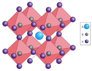
Image Credit: Martin Green et al / Nature Photonics

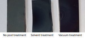
Photographs of CH3NH3PbI3 perovskite films after post treatments: (left) no post treatment; (middle) with solvent treatment; (right) with vacuum treatment.
AFM images of CH3NH3PbI3 layers: with fast crystallization (a), with slow crystallization (b). Perovskite growth and crystallization studied by a surface photovoltage (SPV) technique: spectra of photovoltage (PV) amplitude (c); modulated SPV spectra of in-phase and phase-shifted by 90o signal measured on the layers of CH3NH3PbI3 (d).
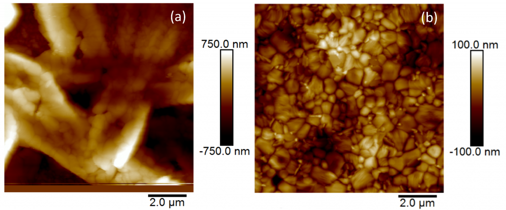
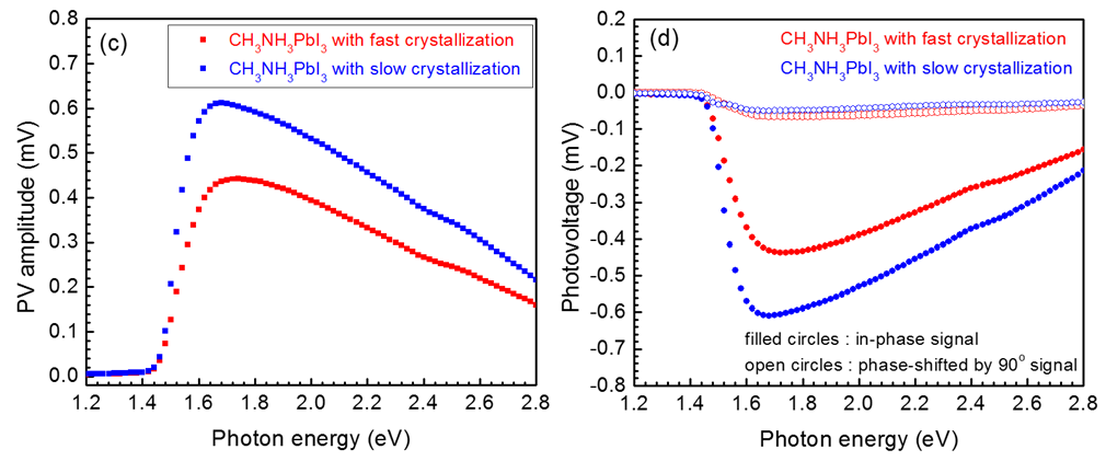
Image Credit: Nakorn Henjongchom